Table of Contents
Open Table of Contents
Introduction
In Electronic System Design 1 class at Northwestern, my partner, Zach Tey, and I designed, programmed, and manufactured a compact embedded webcam setup that streams images through a webserver. The overall embedded design had 3 main components: an Espressif ESP32 microcontroller (called ‘Wifi Chip’ within this report), an Atmel SAM4S8B microcontroller (called ‘MCU’ within this report), and an OVO2640 camera module.
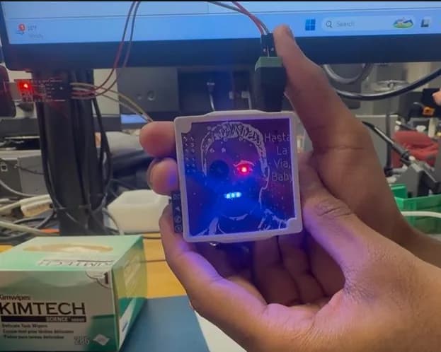
The embedded webcam is laid on a single 50x50 mm PCB including passive components such as bypass capacitors and current-limiting resistors, as well as active components such LED indicators, push buttons, a voltage regulator, and a crystal oscillator. It sits within a physical 3D printed enclosure, and streams images to a wifi server hosted by the Wifi chip.
The camera module captures the images into the MCU, which is then sent via the Wifi chip to a web server coded with Javascript, CSS, and HTML for users to start and stop the webcam at their own leisure. To facilitate the transfer of data, SPI, I2C, and UART protocols were integrated into the communication design to ensure proper handshake procedure and reliable image transfer.
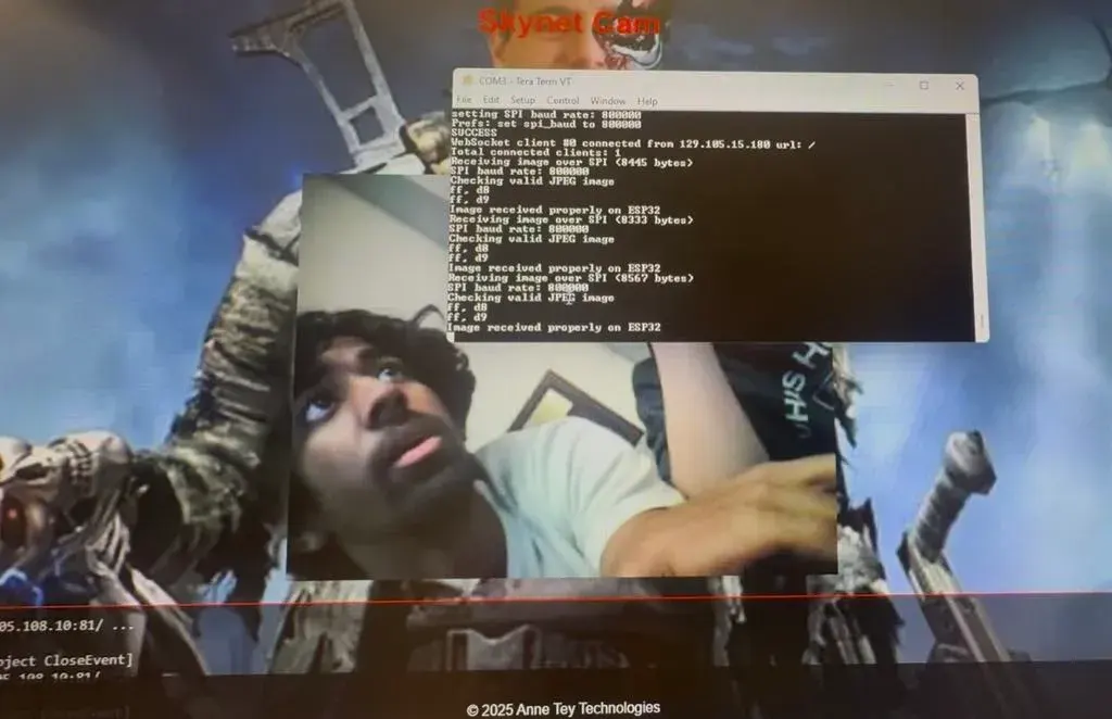
Throughout the process, different software and hardware tools were used to design, debug, and program our final webcam. EAGLE PCB was used to create our PCB schematic and layout, which was eventually produced by JLCPCB. Firmware was competed on Microchip Studio, Atmel’s native programming IDE, equipped with debuggers such as memory maps and breakpoint functionalities. The website front-end was initially outlined on Balsamiq, a wireframing tool, and later designed on Phoenix Code. The CAD design was done through Onshape, and printed on a Bambu Studio 3D printer with its native compatible software. Debugging tools also included the Logic Analyzer, Tera Term (a serial communication output monitor), as well as old school multimeters.
This post aims to explain in-depth the mechanics and operation of the actual project, the design process of each step, challenges we faced along the way, reflections on teamwork, and a summary of key learnings.
Design Process
PCB Design
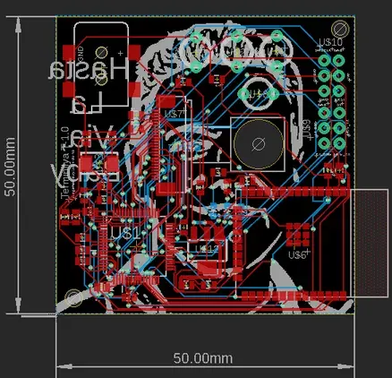
The PCB design was critical to the project’s success, as it electrically integrated all necessary components onto a compact layout for efficient hardware and software interaction. We developed a two-layer PCB using EAGLE, condensing the functionality originally tested on a breakout board. Throughout the schematic development, we cross-referenced our design against the original breakout schematic, provided to us by our professor, preserving essential connections, clarifying component naming, and eliminating unnecessary header pins and redundant traces.
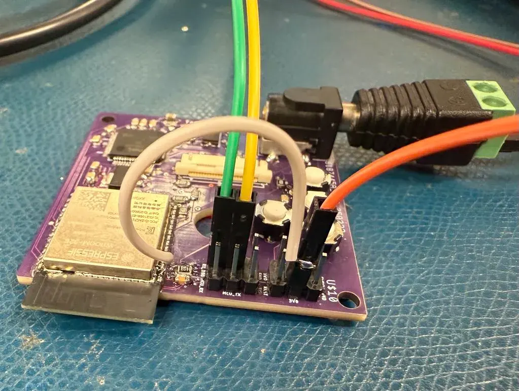
Ensuring comprehensive component integration was essential due to our board’s complexity beyond the main microcontrollers and camera header. We utilized a 5V barrel jack as our power source, stepped down to 3.3V via a voltage regulator to power the ESP32. Four SPST push buttons were implemented: two for ESP32 programming (IO1 and EN), one for asynchronously resetting the MCU, and another for Wi-Fi provisioning. Three LEDs were added for debugging, along with a 16 MHz crystal oscillator for the MCU’s phase-locked-loop operation. Header pins facilitated board programming and enabled oscilloscope connections during debugging. Determining which connections to include or omit was notably challenging.
The board layout was constrained to a 50x50 mm area, incorporating physical mounting points and mechanical considerations. The barrel jack was oriented outward to enhance mechanical integration. Electrically, bypass capacitors were placed near microcontroller pins, and a comprehensive ground pour was added post-routing to ensure a low-impedance return path. Creatively, we enhanced the board’s aesthetic by incorporating a customized silkscreen featuring a modified image of our professor as the Terminator (T-800). The camera lens aligned perfectly with the Terminator’s eye, and LEDs aligned with the character’s teeth. This unique design required careful component placement to ensure all essential electronics were confined to one side of the PCB, leaving space for our artistic silkscreen.
I learned the benefits of formatting and organization of my schematic to be labeled clearly with net-labels, allowing for readers, and myself, to clearly debug and understand the electrical connections made, instead of cluttering the screen with wires and lines. I also took into consideration mechanical limitations such as the direction of the barrel jack, the order of the header pins, the size and location of mounting holes, the orientation and readability of silkscreen text, and ensired sufficient spacing between electrical components.
MCU Firmware
The firmware design process for the SAM4S8B-based camera system involved creating and modifying several key files to manage communication between the MCU, the ESP32, and the OV24640 camera module. The development was divided into three main sections: WiFi communication, camera control, and overall system initialization and operation.
For WiFi communication, the wifi.c and wifi.h files were implemented to handle UART and SPI communication with the ESP32. The wifi.c file included functions for initializing WiFi variables, configuring USART and SPI interfaces, and handling incoming data through interrupt service routines. The handlers processed incoming bytes, managed command responses, and initiated provisioning mode when triggered by an external button. In provisioning mode, the ESP32 creates a temporary WiFi access point, allowing nearby devices to connect and access a web interface. Through this interface, users can enter the desired network credentials (SSID and password). Once submitted, the ESP32 stores the credentials in its memory and attempts to connect to the specified network.
To initiate provisioning, we configured the SAM4S8B to trigger the mode through a button press interrupt. When activated, the SAM4S8B sends a command to the ESP32, placing it into provisioning mode. After the ESP32 successfully connects to the specified network, it signals the SAM4S8B by setting a GPIO pin high, confirming that provisioning was completed. This implementation allows the system to dynamically connect to different networks without requiring hardcoded credentials.The SPI interface was configured to transfer image data from the MCU to the ESP32 in chunks, with proper acknowledgment handling through rising-edge interrupts.
For camera control, the camera.c and camera.h files managed the OV2640 module. Several functions were created to initialize the camera pins, configure the two-wire interface (TWI), and set up parallel capture. Image acquisition was triggered by the VSYNC rising edge, with the image data stored in a buffer. The system processed JPEG images by identifying the start and end markers (ffd8 & ffd9) to determine the image length. The camera was configured to operate at 320 × 240 resolution using a sequence of OV2640 register settings.
The main program in main.c orchestrated the overall system operation. It performed the initializations for the clock, board, WiFi, camera, and interrupts. The main loop continuously checked for provisioning requests, handled network availability, captured images, and transferred them to the ESP32 over SPI when clients were connected. Error handling mechanisms were added, such as resetting the WiFi module and retrying the connection if the expected “SUCCESS” response from the ESP was not received. Supporting files like conf_board.h, conf_clock.h, and init.c defined board-specific pin configurations, clock settings, and initializations. We also utilized external libraries (asf.h through the ASF Wizard portal) and included additional files for the camera driver (ov2640.c/h) and timer interface management that were provided through some example code.
Throughout the development, we attempted to follow best practices, including marking interrupt-modified variables as volatile, including necessary header files, and disabling compiler optimization for easier debugging.
Webserver
Our website was developed using HTML, CSS, and JavaScript. HTML provided the structural layout of each webpage, CSS handled the formatting and design aspects, and JavaScript was responsible for implementing the webcam’s streaming functionality. Each webpage utilized a dedicated CSS file, with JavaScript primarily integrated into the webcam streaming page (webcam.html). The website includes three primary pages: index.html, webcam.html, and info.html.
The index page welcomes users with basic information about our project and a visual of our PCB. The webcam page allows users to start and stop the camera stream via a button, utilizing JavaScript event listeners and websocket connections to communicate directly with the ESP32. Additional features on this page include real-time timestamp and frame rate indicators, and a log display for debugging purposes. Finally, the info page provides brief personal biographies and contact information. For website hosting, we initially used Balsamiq to wireframe the site structure, then implemented it using Phoenix Code. HTML/CSS files were developed and modified using VSCode with the PlatformIO extension, which facilitated rapid updates directly to our server.
We decided to continue along with the Terminator theme of the entire project. Since our professor encouraged us to make it “as annoying as possible”, we decided to embed a trivia game to prompt the user to answer several questions as “fill in the blank” style movie quotes from the Terminator movie. If the user inputs an incorrect answer, the screen will automatically transition to a 3x3 matrix whack-a-mole style game, where the user will have to click on the image of Professor Mikhelson out of the nyan cat array to return to the webcam page. If the user does not do so, the array will increase in step sizes of 1 (3x3 to 4x4…), until it reaches a 20x20 array. If the user still does not pass the game, the user will be directed to a page where a countdown timer starts, and will receive a ‘failed game’ animation.
Below is an embedded HTML version of our webserver. Of course, you don’t have the physical webcam in front of view, so the webcam functionality will not work, but alas, you can appreciate the UI/UX.
CAD Enclosure
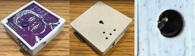
The enclosure was designed in Onshape to meet the specified requirements, featuring a fully enclosed structure with wall thickness of 1.5 mm to ensure durability. We decided to opt for a ‘snap fit’ assembly, where we didn’t require any standoffs or screws to hold the pcb in place within the enclosure. Instead, ‘pins’ were added to the casing to allow for the pcb to slot in place, and an external compliant snap-fit was designed to secure the pcb and casing to the rest of the mount. Cutouts were included for the Wifi chip antenna, barrel jack power supply, and small access holes for the MCU reset and WiFi provision buttons, allowing them to be pressed with a pin. The front face of our pcb, featuring a silkscreen ‘TerminIlya’, as well as our led indicators (power and otherwise) was exposed through a cut out of the lid.
Additional holes were created for the indicator and power LEDs, ensuring they remain visible without opening the enclosure. The back panel incorporated a single mounting hole, allowing the enclosure to be mounted to a wall with the camera facing forward and properly oriented for an upright video stream. The necessary clearances were employed to allow for the longer camera module to fit inside the case snuggly, without crimping the wire.
Integration
Integrating our final PCB and firmware presented challenges, although fewer than anticipated. One significant issue involved the inability to power the board at first power-up. This issue was traced using a multimeter to an incorrect naming of the 3.3V pins in our schematic. We resolved this by soldering a jumper wire.
Another critical issue was the failure to read the correct device signature when connecting via J-Link to Microchip Studio. After extensive debugging with a multimeter, we discovered a solder bridge on the camera header that shorted the 1.2V and 5V power rails. This short damaged the MCU chip, preventing proper device recognition. We resolved this by obtaining a replacement MCU chip, correcting the soldering issue, and reassembling the board.
These two challenges showed us the importance of being meticulous with our work, even in the miniscule details, down to the very last solder bridge, that could cause an entire system to fail.
Reflection
Professor Mikhelson’s teaching made it one of the best classes I’ve taken at NU so far! While I came in with some background on PCB design, I’ve never used Atmel Studio. Working with low-level peripheral configuration through ASF and CMSIS gave me a deeper appreciation for embedded systems programming outside the STM32 ecosystem. If you are at NU and want to learn more about the class from a student’s perspective, feel free to reach out!