Hi! This was my final oral for EE495 (Spring 2025), an introductory class on nanophotonics, at Northwestern University. Students were tasked to find a relevant paper in the field and present an oral on it. Specifically, my prompt was to
- Pick 1 paper in plasmonic material and device area and describe the main goals and key results of the paper
Of course, I was too nerve-wracked to remember to record my presentation, so you’ll have to make do with this post :). Here’s my presentation file:
Table of Contents
Open Table of Contents
Introduction
Guiding light at the nanometer scale is a central challenge in nanophotonics. Conventional dielectric waveguides and photonic crystal structures are limited by the diffraction limit, confining light only on the order of a wavelength in at least one dimension. For example, dielectric nanowires or silicon photonic wires can confine light strongly inside a high-index core, but as dimensions shrink below , a significant fraction of light leaks into the surroundings, and confinement remains diffraction-limited in at least one transverse dimension.
Surface plasmon polaritons (SPPs) at metal-dielectric interfaces, on the other hand, allow subwavelength localization of fields at optical frequencies by binding light to oscillations of conduction electrons at the metal surface. However, SPP modes in simple configurations suffer high ohmic losses in the metal and, in “long-range” SPP designs, their confinement is often poor (comparable to dielectric waveguides) due to distributing the mode over a wider area to reduce loss. The net result is a trade-off: tighter confinement generally comes at the expense of increased propagation loss.
A promising solution is to hybridize dielectric waveguiding with plasmonics. In a seminal work, Oulton introduced a hybrid plasmonic waveguide that combines a semiconductor nanowire with a metal surface separated by a nanoscale dielectric gap. This hybrid waveguide effectively merges a conventional dielectric waveguide mode with a SPP mode, producing a new guided mode with both deep subwavelength confinement and relatively long propagation distance. The hybrid mode was shown to be tightly confined to an area more than smaller than the diffraction-limited spot (in free space) while maintaining propagation lengths exceeding those of pure SPP modes on a comparable interface. By adjusting the geometry (nanowire size and gap thickness), the propagation distance can be increased to the millimeter range while still keeping moderate subwavelength confinement. This approach extends the capabilities of both plasmonics and semiconductor photonics, enabling truly nanoscale optical interconnects and paving the way for subwavelength lasers (e.g. visible nanolasers and terahertz quantum cascade lasers) and other integrated nanophotonic devices.
In this post, I aim to explain the hybrid plasmonic waveguide with a focus on theoretical modeling and mathematical detail. We outline the physical structure and derive key equations describing its guided modes, including the effective index formulation, mode hybridization via coupled-mode theory, and calculations of mode area and propagation length. We then discuss the results of these analyses, which illustrate how the hybrid mode transitions between “cylinder-like” (dielectric waveguide) and “SPP-like” extremes and achieves superior performance compared to other plasmonic waveguides. Potential applications and future outlook of hybrid plasmonic waveguides are also presented. For completeness, the appendix provides a brief estimation of surface plasmon resonance frequencies for relevant metal/dielectric interfaces.
Theoretical Background
Light propagation in a waveguide can be described by a modal eigenvalue equation obtained from Maxwell’s equations. For a translationally invariant structure (invariant along the waveguide -axis), we seek modes with electric and magnetic fields and , where is the propagation constant and the angular frequency. The mode has an effective refractive index , where is the free-space wavenumber. The effective index lies between the refractive indices of the constituent materials and reflects the fraction of the mode in each region.
In a dielectric waveguide (such as a high-index nanowire in a lower-index surrounding), the mode primarily resides in the high-permittivity core and decays evanescently outside. The confinement is limited by the core size and index contrast. If the core diameter is much larger than the wavelength, the mode is well confined; as the core shrinks to subwavelength dimensions, a significant portion of the field extends into the cladding (air or dielectric), thereby enlarging the effective mode area.
In a metal-dielectric interface supporting an SPP, the mode is confined near the interface within a skin depth of the metal and an exponential decay into the dielectric. The SPP effective index for a planar interface between a metal (permittivity ) and a dielectric (permittivity ) is found from the dispersion condition . Thus the SPP mode index is
which for (metallic behavior) yields , indicating the SPP mode travels slower (higher phase delay) than light in the dielectric. The field is tightly confined to the interface if is large, but importantly, part of the energy resides in the metal, leading to significant attenuation because at optical frequencies (ohmic loss). Long-range SPP configurations (such as symmetric metal/dielectric multilayers) spread the mode over a wider cross-section to reduce field intensity in the metal, which lowers loss but also greatly increases the mode area, losing the nanoscale confinement advantage.
To quantify mode confinement, we define the modal electromagnetic energy density and the total energy per unit length . A general expression for time-averaged energy density in a dispersive medium is
which reduces to the familiar for non-dispersive, lossless materials (where ). The total mode energy (per unit length along ) is integrated over the entire cross-section. We can then define an effective mode area as the ratio of total energy to the peak energy:
This has units of area and intuitively represents the cross-sectional area that the mode would occupy if the energy were uniformly distributed at the peak density . A smaller indicates tighter confinement of the field. It is often useful to compare to a reference diffraction-limited area; following Oulton, we can define (the area of a square) and use as a normalized mode.
Another key metric is the propagation length , which we take as the distance over which the power of the mode decays to of its initial value. If (with for lossy modes, since fields decay as ), then
Modes with lower loss (smaller ) have longer . Pure dielectric waveguide modes typically have negligible (dielectrics can be very low loss at optical frequencies), whereas plasmonic modes have significant due to absorption in the metal.
So, achieving deep subwavelength confinement together with long propagation requires balancing two opposing tendencies: concentrating the field into tiny regions (like a gap or metal surface) increases and thus reduces , but it typically also increases the field overlap with absorbing materials (metal) or introduces other loss, thereby increasing and reducing . The hybrid plasmonic waveguide is engineered to strike this balance by mixing a low-loss dielectric mode with a highly confined plasmonic mode. In the next section, I’ll describe the structure and develop a mathematical model for this hybridization.
Design and Mathematical Model
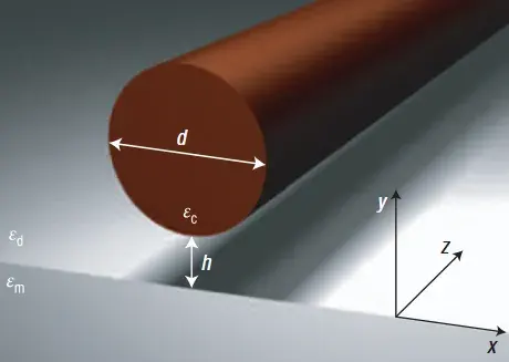
The hybrid plasmonic waveguide considered here consists of a high-index semiconductor nanowire (or nanorod) placed in close proximity to a flat metal surface with a thin low-index spacer in between. A schematic cross-section of the geometry in the below image. The nanowire of diameter and permittivity (for example, GaAs with at ) sits above a metallic half-space (e.g. silver) with permittivity (for Ag at 1550~nm, ). Separating the two is a nanoscale dielectric gap of thickness and permittivity (e.g. a silicon dioxide layer, ). The upper cladding above the nanowire can be air or another dielectric (here we assume a symmetric top cladding also of permittivity for simplicity). The coordinate origin is taken at the center of the nanowire.
Schematic of the hybrid plasmonic waveguide geometry (not to scale). A high-index semiconductor nanowire (permittivity , diameter ) is separated from a metal substrate (permittivity ) by a thin low-index dielectric gap (permittivity , thickness ). The hybrid guided mode (red intensity profile) is confined in the gap and the nanowire, taking on characteristics of both a dielectric waveguide mode and a SPP mode at the metal surface. (From R.F. Oulton et al. (Nature Photonics, 2008))
Physically, this structure allows the mode of the nanowire (which by itself would mostly reside in the high-index core) to couple evanescently across the gap and interact with the SPP mode bound to the metal surface. The dielectric gap is small enough (on the order of a few tens of nanometers or less) that the evanescent tail of the nanowire mode significantly penetrates into the gap and can drive charge oscillations on the metal, while still preventing the nanowire from contacting the metal (which would introduce high loss directly). The configuration is fully compatible with semiconductor fabrication techniques since it essentially involves placing a nanowire on a metal-coated substrate with a thin insulator spacer.
To analyze the guided modes of this hybrid structure, one can use numerical solutions of Maxwell’s equations (for example, finite element method as done in Oulton) to find , , etc. However, much insight can be gained from a simplified analytical model using coupled-mode theory. In this approach, we treat the hybrid mode as arising from the coupling of two “basis” modes: (i) the fundamental mode of the isolated nanowire (with no metal present), having an effective index , and (ii) the SPP mode of the metal-dielectric interface (with no nanowire), having index given by Eq. 1. These two modes are phase-matched to some degree and can exchange energy through the overlap of their fields in the gap region. When brought into resonance (i.e. when ), strong hybridization occurs.
Following coupled-mode theory, we can set up a eigenvalue problem for the hybrid mode index . Let denote the coupling coefficient (with dimensions of refractive index) between the nanowire mode and the SPP. The characteristic equation can be written as:
This is a quadratic equation whose solutions are the effective indices of the two hybrid eigenmodes (a symmetric "" and an antisymmetric "" combination of the basis modes). Solving Eq. 5 yields
where corresponds to the higher-index (usually bonding) hybrid mode and to the lower-index mode. The mode of interest in this work is the symmetric/bonding mode (often simply denoted ) because it tends to concentrate energy in the gap (like a parallel-plate capacitor) and has lower loss than its antisymmetric.
The normalized amplitude of the nanowire-mode component in the hybrid mode can be found from the eigenvector of Eq.~\eqref{eq:charpoly}. If we write the hybrid mode field as
with and being the modal amplitude coefficients (normalized such that ):
This quantity indicates the fraction of the hybrid mode that is “cylinder-like”, whereas is the fraction that is “SPP-like”. When , the mode is dominated by the dielectric waveguide character, and when , it is more plasmonic in nature. At the critical diameter where , the coupling is symmetric; we have midway between and , and the hybrid mode comprises equal parts of each basis mode ().
For the hybrid waveguide under study, typical material parameters at are as given above (GaAs or similar high-index nanowire, silica gap, silver metal). Using , , and in Eq. 1 yields (mostly real part, since is small). The uncoupled nanowire mode index will vary between about (for very small , the mode mostly in silica) up to (for large , approaching a bulk-like index). Thus, for a certain intermediate diameter , one expects ; indeed Oulton found for their structure.
Note emphasize that Eqs. 6 & 7 provide qualitative understanding; for quantitative results (especially including the loss, which enters ), numerical solutions are used. In the following section, we summarize key results for , mode area , and propagation length as functions of the geometry, and discuss how they reflect the hybrid nature of the mode.
Key Results and Interpretation
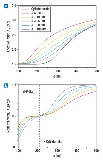
The hybrid waveguide mode exhibits a continuous transition between a dielectric-like regime and a plasmonic regime as the nanowire diameter and gap width are varied. Figures 2a and 2b illustrate this behavior by plotting the effective index and the mode character (cylinder fraction) as a function of for several representative gap thicknesses . For large nanowire diameters (~nm), approaches (the black curve in Fig. 2a), and approaches 1 (Fig. 2b), indicating a \emph{cylinder-like} mode dominated by the dielectric waveguide core. In this regime, the metal plays a negligible role; the mode is essentially confined in the nanowire with low loss, and the propagation length is very long (limited only by any absorption in the dielectric). On the other hand, for very small diameters (), approaches (horizontal dashed line in Fig. 2a) and (Fig. 2b), indicating an SPP-like mode. In this regime, the nanowire is too small to confine the mode effectively, and the mode spreads out along the metal surface with only weak localization around the wire; consequently the confinement in the direction along the metal surface is poor and the loss is high (comparable to an uncladded SPP).
At intermediate diameters around , the hybrid mode most strongly blends both characters. In Fig. 2a, one can see an avoided crossing behavior: as increases, (black line) approaches (dashed line), but the hybrid mode indices (colored lines) split and repel from the crossing point due to coupling. The upper branch is significantly higher than either uncoupled index in this regime, a typical signature of hybridization (the mode is more tightly bound than either individual mode alone). Meanwhile, Fig. b shows that transitions through 0.5 near this diameter, confirming that the mode goes from being mainly SPP-like to mainly dielectric-like. The strongest coupling occurs near this balanced point (~nm for small ), which correlates with a notably \emph{small} mode area but also a reduction in propagation length (due to increased field in the metal). Essentially, at resonance the energy is concentrated in the nano-gap between the wire and metal, maximizing the effective optical capacitance.
_Figure 2: Hybrid mode effective index and composition vs. nanowire diameter, from coupled-mode analysis (color curves) and analytical limits. Effective index of the hybrid mode as a function of nanowire diameter for various gap widths (colored solid lines). The black solid line is for an isolated dielectric nanowire (no metal), and the black dashed line is for a metal/dielectric interface (no nanowire). Corresponding weight of the nanowire (cylinder) mode in the hybrid mode. By definition, means the mode is cylinder-like and means SPP-like. The vertical grey line marks the critical diameter where (here ~nm), at which point (equal mix of both modes). (From R.F. Oulton et al. (Nature Photonics, 2008))_
The influence of the gap thickness is also critical. A larger gap ( on the order of hundreds of nm) weakens the interaction between the nanowire and the metal, thus becomes small and the modes remain mostly separate: the hybrid mode stays closer to whichever basis has higher index at that . In contrast, as shrinks to just a few nanometers, grows and the coupling becomes very strong. In the extreme case of (nanowire almost touching metal), one would expect the hybrid mode to become extremely confined in the gap (approaching a parallel-plate capacitor mode) with dramatically small , while would tend toward that of a metal-semiconductor surface plasmon (since ultimately much of the energy lies at a metal-semiconductor interface). Oulton notes that for very small on the order of a few atomic layers, quantum mechanical effects and nonlocal dielectric response of the metal would come into play, which are beyond the local classical model.
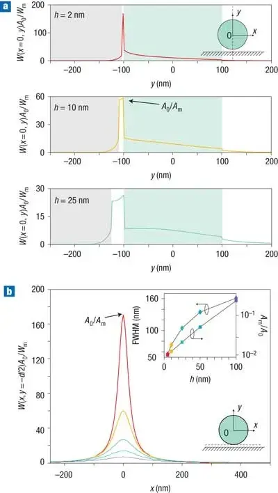
Figure 3 provides further insight by plotting the electromagnetic energy density distributions for selected cases. Panel (a) shows the normalized energy density along a vertical cut through the gap for different gap sizes , highlighting how the field localizes in the low-index gap region. For a large gap (e.g. ~nm, green curve), the field spreads out and decays slowly into the dielectric; for a moderate gap (~nm, gold curve) the field is more confined; and for an ultra-narrow gap (~nm, red curve) the energy is sharply peaked at the metal-dielectric interface. Panel (b) shows along a horizontal line through the gap (just under the nanowire) for the same cases, demonstrating subwavelength confinement in the lateral direction as well. Even for the most confined case (~nm), the propagation length of the hybrid mode was found to \emph{exceed} that of an SPP on a corresponding metal-semiconductor interface, thanks to the fact that a substantial fraction of the mode energy (though confined tightly) resides in the dielectric gap rather than inside the metal. In other words, the gap region stores oscillating electric energy like a capacitor, reducing the dissipative loss compared to a conventional SPP which has more field penetrating into the metal.
Figure 3: Electromagnetic energy density profiles for the hybrid mode, showing subwavelength field confinement in the gap region (for several gap widths ). vs. vertical position (with at nanowire center), plotted for gap ~nm (red), ~nm (orange), and ~nm (green). The shaded gray and green areas denote the metal and semiconductor regions respectively; the unshaded region is the low-index gap. The peak near the metal surface (at , just above the metal) becomes sharper and stronger as decreases, indicating tighter -confinement and higher energy density for smaller gaps. vs. horizontal position (cut through the middle of the gap beneath the nanowire) for the same three gap values. The mode width (full-width at half-maximum, FWHM) in the -direction is deeply subwavelength (tens of nm or smaller). The inset in (b) shows the FWHM in (vertical confinement) and the normalized mode area as functions of . As shrinks, the mode area drops (approaching or lower) while confinement tightens. (From R.F. Oulton et al. (Nature Photonics, 2008))
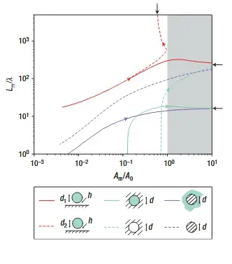
Perhaps the most significant outcome is that the hybrid waveguide outperforms other plasmonic waveguide geometries in terms of the trade-off between confinement and propagation. Figure 4 plots normalized propagation length () against normalized mode area () for a variety of plasmonic waveguides reported in literature. Curves are shown for the hybrid mode (red) as well as, for example, dielectric-clad metal nanowires (blue) and metal-coated dielectric nanowires (green). Each curve represents how and change as a structural parameter is varied (for the hybrid, varying from very small to large; for the other cases, varying their core sizes). In this log-log plot, the upper left corner corresponds to long propagation and strong confinement (a very desirable but difficult combination), whereas the lower right corresponds to short propagation and weak confinement (undesirable). The hybrid waveguide’s trajectory lies toward the top-left compared to the others, indicating a clear performance advantage. For a given mode area, the hybrid mode propagates an order of magnitude farther than other plasmonic modes; equivalently, for a required propagation length, the hybrid mode can provide much tighter confinement. In particular, in the regime of deep subwavelength areas ( to ), the hybrid design offers on the order of — wavelengths, whereas alternatives are often limited to or less. This remarkable balance is what makes the hybrid plasmonic waveguide so attractive for nanoscale photonics.
Figure 4: Comparison of various plasmonic waveguides in terms of normalized propagation length vs normalized mode area . Each curve represents a family of modes as a structural parameter is varied. The red curve is the hybrid plasmonic waveguide (varying gap for two fixed diameters ~nm and ~nm). Blue curves correspond to dielectric-cladded silver nanowire modes, and green curves to silver-coated dielectric nanowire modes (data from Refs.~4—6 in \cite{Oulton2008}). Arrows indicate the direction of increasing coupling (decreasing gap or increasing overlap) along each trajectory. The gray shaded area on the right indicates the approximate diffraction-limited size scale ( and larger). The hybrid mode clearly extends further toward the top-left (small , large ) than the other waveguides, demonstrating an order-of-magnitude improvement in the confinement-propagation trade-off. (From R.F. Oulton et al. (Nature Photonics, 2008))
In summary, the key results from Oulton’s analysis are:
- The hybrid waveguide supports a deeply subwavelength mode confined in the nano-gap between the wire and metal, with modal area reaching down to (over smaller than a diffraction-limited spot) in certain configurations.
- At the same time, propagation distances on the order of — micrometers (tens of wavelengths) are achievable, which is significantly longer than typical SPP modes of similar confinement. By adjusting geometry, can even approach the millimeter scale if one is willing to relax confinement somewhat (e.g. larger ).
- There is an optimal coupling point (around ~nm for the studied example) where the mode is an even hybrid of dielectric and plasmonic nature, corresponding to maximum field concentration in the gap. This yields the smallest but also incurs higher loss; slightly off this point, one can trade a small increase in for a big gain in .
- Compared to other plasmonic waveguide designs (metal stripes, wedges, nanowires, etc.), the hybrid waveguide offers a superior compromise between and , effectively expanding the achievable design space for nanoscale guided waves.
The underlying reason for these favorable properties is that the hybrid mode stores a significant portion of its energy in the low-loss dielectric gap (as electric field) while still exploiting the metal’s ability to confine the field tightly. The gap region acts analogously to a nano-scale capacitor, capturing energy in the electric field between the metal and semiconductor. This mitigates the participation of the metal in carrying the energy (thus reducing loss) even as the presence of the metal helps squeeze the field into a subwavelength volume. The result is a guided mode that is both nano-confined and relatively low-loss.
Discussion
The hybrid plasmonic waveguide platform opens up several exciting possibilities in nanophotonic device engineering. One immediate application is in the development of nanoscale lasers (“nanolasers”). By incorporating a gain medium into the semiconductor nanowire, the hybrid mode can provide the optical feedback and mode confinement needed for lasing at deeply subwavelength scales. Indeed, following the proposal of Oulton et al., demonstrations of hybrid plasmonic nanolasers at visible and near-infrared wavelengths have been achieved (using semiconductor nanowires as gain media atop metal substrates). These devices, sometimes called “spasers” or plasmonic nanolasers, can generate coherent light with mode volumes far below the diffraction limit, useful for on-chip optical sources, sensors, and non-linear optics where strong light-matter interaction is desired.
Another application area is integrated photonic circuits. Hybrid plasmonic waveguides can serve as ultra-compact interconnects between photonic components, acting as a bridge between dielectric waveguides (which have low loss but larger mode size) and nanoplasmonic elements (which have ultrasmall size). For example, one could envision routing signals in a silicon photonic circuit and then coupling them into a hybrid plasmonic section to achieve a tight bend or modulation in a nanoscale region, and then back to a dielectric waveguide. The relatively long propagation distance of hybrid modes (tens to hundreds of microns) means they can cover useful distances on a chip without regeneration. Moreover, since the hybrid waveguide is fundamentally a metal-dielectric structure, it could be integrated into electronic-photonic circuits where the metal part can also carry electrical bias or form part of a device electrode.
The hybrid approach is general and can be adapted to different material platforms. While the original work used GaAs and silver at telecom wavelengths, later studies have explored silicon nanowires on silver for near-infrared, or ZnO nanowires on Ag for ultraviolet, etc., each benefiting from the same principles. Alternative geometries like hybrid plasmonic slots, wedges, and ring resonators have been proposed and analyzed, indicating that hybridization can improve figures of merit across a range of plasmonic waveguide types. Additionally, if the metal loss remains an issue, one could incorporate gain media in the dielectric to partially or fully compensate the loss, potentially enabling lossless or even amplifying plasmonic propagation.
Looking forward, one interesting direction is to explore the ultimate limits of confinement with hybrid modes. The current model assumes classical electromagnetic behavior even for nanometer and sub-nanometer gaps. At such small scales, quantum effects such as electron spill-out and nonlocal response in metals, as well as quantum tunneling, can alter the plasmonic response. Accounting for these will be necessary for predicting behavior in extreme confinement (few-nm gaps). Another consideration is fabrication: assembling or patterning the required structures with nm precision is challenging, but advances in bottom-up nanowire growth and transfer, as well as top-down lithography, are making hybrid waveguides feasible in practice. The compatibility of this design with standard semiconductor processes is a big advantage, as it does not require complex shapes in the metal (a simple film is satisfactory).
All in all, these waveguides are rad.
Appendix: Estimation of Surface Plasmon Resonance Frequencies
Surface plasmons at a single metal-dielectric interface exhibit a characteristic resonant frequency at which the SPP mode becomes non-propagating (the wavevector ). This occurs when the real part of the metal’s permittivity cancels that of the dielectric. For a metal with a Drude-like permittivity (neglecting damping for simplicity), the condition yields
where is the bulk plasma frequency of the metal. For a metal/air interface (), this simplifies to . For example, silver has ; with (silica cladding), Eq. 8 gives (roughly 250 nm in wavelength). At frequencies (longer wavelengths), and SPPs can propagate along the interface with a finite given by Eq. 1. As approaches from below, increases (light slows down and the mode becomes more confined to the interface). Beyond , becomes negative and the SPP mode no longer exists as a bound mode (instead one gets a screened plasma oscillation). In the context of the hybrid waveguide, the operating frequency is typically well below of the metal used (for instance, 1550 nm is for Ag, much lower than ), ensuring that SPPs are supported. The concept of is useful when choosing metal and wavelength: one generally wants somewhat below so that the metal still has a large negative permittivity (for strong confinement) but not too close to to avoid excessive loss (which tends to increase near plasmon resonance).