This post is about some simulations I learned to make over the past couple of weeks. Check out my the part 1 post for a more detailed overview of the topic, but I’ll be providing context here as well. This is my first time attempting to embedd Julia simulations in my portfolio, so bear with me. All of the assumptions I made (apart from a couple, which are noted) are based of off R.F. Oulton et al. (Nature Photonics, 2008).
Table of Contents
Open Table of Contents
Structure of the HPW
A hybrid plasmonic waveguide (HPW) consists of a high-index dielectric waveguide placed very close to a metal surface with a thin low-index space (gap) in between. In the case I’ll be studying , the strucutre is a silicon (Si) nanowire (high permittivity) seperated from a flat silver (Ag) substrate by a nanoscale silicon dioxide (SiO2). Light is guided by the hybrid mode that arises from coupling the dielectric waveguide mode in the Si core and the surface plasmon-polariton (SPP) mode at the metal surface. This coupling concentrates the electromagnetic energy in the gap region (like a capacitor) between the metal and dielectric. The benefit is a deep-subwavelegnth confinitement, where the mode area can be 50-100 times smaller than the diffraction limit, while much of the field resides in the dielectric, resulting in lower ohmic losses.
The tradeoff, however, is small gaps increase propagation loss. For example, with a very thin gap (h = 5 nm), the mode area can be , but propagation lengths drop to tens of microns. With larger gaps, the confinement is weaker (~), but propgation lengths are upwards of
Geometry and parameters
In my simulation, I modeled a Si nanowire of diameter sitting on a SiO2 film of thickness above a ‘thick’ silver substrate (basically an ‘infinite’ metal with respect to other length scales). The nanowire in the cross-section is treated as a cylinder of diameter (or an equivalent square cross-section). The gap is the SiO2 thickness seperating the nanowire’s bottom from the metal. The simulation domain is the 2D cross-section (x-y plane) as shown below, with the z axis (into the screen) being the propagation direction. Outside the Si wire and gap, I take the surrounding medium to be air for simplicity (n ≈ 1).
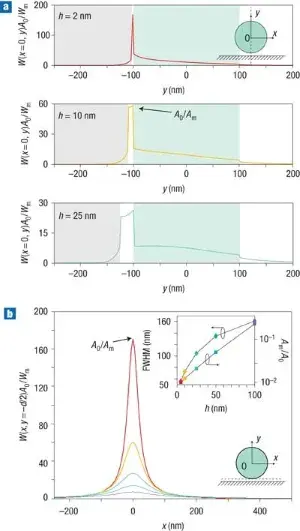
Simulated cross-section field profile of the fundamental hybrid mode (power density W at x=0) for different gap sizes (h = 2, 10, 25 nm). The Si nanowire (green circle, diameter d) sits above an Ag substrate (gray) with a thin SiO₂ gap (white). The field is tightly confined in the nanoscale gap, with smaller gaps yielding higher peak intensity in the gap.(From R.F. Oulton et al. (Nature Photonics, 2008))
Operating wavelenght
I allowed the free-space wavelength in vacuum to be varied (for example, around telecom 1550 nm). This actually affects the metal’s permittivity and the mode properties (see below).
Material Models:
I need to use realistic frequency dependent permittivities. For silver (Ag), I did some research to find that a dispersive model is the most relevant. This is because silver’s optical resonance varies strongly with frequency, and this behavior is not well captured by constant permittivity. I found an optical constants model (Johnson & Christy 1972 data), or I could use the Drude/Lorentz model (I am currently reading through Ashcroft & Mermin’s Solid State Physics, will be making notes soon)!
The MaxwellFDFD.jl package conveniently includes built-in frequency dependent dielectric constants for common materials in nanophotonics from standard references! So, we can obtain for Ag at the selected (for example, at = 1550 nm, silver’s permittivity is about ). For Si, I assumed constant index since it varies slowly in IR - e.g. at m (). For the silica dielectric, I used at m (). I think that using a fixed n for the dielectrics is a good approximation, mostly since I was a bit lazy to interpolate between data.
Simulation Tools + Approach
I built the simulatino in Julia using open-source EM solvers. Here’s a list of important tools:
- MaxwellFDFD.jl / FDFD.jl: Finite-Difference Frequency-Domain solvers for Maxwell’s equations. These libraries let me define a 2D or 3D geometry on a grid and solve for the E and H fields in frequency domain subject to boundary conditions. I have no clue how these work!
- MaxwellFDFD provides some high-level routines (like maxwell_run) and features like waveguide mode solvers, dispersive materials, and PML boundary conditions.
- FDFD.jl is a pure-Julia 2D FDFD implementation which, together with FDFDViz.jl, allows custom setups and plotting. I found some notes from EE256.
- Pluto.jl: a cool Jupyter like environment that provides a reactive environment for interactive simulations. The output simulations you see on my post are direct embeddings of HTML that Pluto generates.
- GLMakie.jl: graphics library in Julia!
Discretization
I defined a grid (spacing of 5nm) over the cross section. This is fine enough to resolve the ~10nm gap and fields. I surrounded the structure with PML (perfectly matched layer) absorbing boundaries to simulate an open domain. The metal substrate is treaded as occupying y < 0. I used a PML thickness of 100 nm (which is just 20 grid cells) at each boundary. In FDFD.jl, the Grid can be defined with PML cell counts (like grid = Grid(Δ, [N_pml_x, N_pml_y], [x_min, x_max], [y_min, y_max])).
Geometry Setup
- The silver region covers the substrate (e.g. a rectangle spanning the entire x-range from y = –metal*thickness to y = 0, or simply all y < 0). I specified two Box objects to represent the semi-infinite metal on either side of the nanowire. In FDFD.jl, I set a region of the grid with for y < 0.
- For the silica gap, I used a rectangle spanning y = 0 to y = h. The SiO2 is extended laterally across the entire domain. is assigned here!
- The Si nanowire is defined as a cylinder of diameter d, whose bottom sits at y = h. is assigned here!
- Everywhere else, I treated as background (leaving it as air, so is 1).
Guided Mode (Frequency-Domain Solution)
To obtain the modal fields nad the propagation constant, we first solve for Maxwell’s equations in the frequency domain for a guided mode solution. In a frequency-domain approach, we should first look for the E(x,y) and H(x,y) fields that satisfy the source-free Maxwell curl equations with some assumed propgation. For example, we can let . This leads to an eigenvalue problem for . MaxwellFDFD.jl includes a waveguided mode solver for this purpose, and FDFD.jl can compute modes by excitingb a mode source. I chose to use FDFD.jl:
Mode Excitations:
I set up a small simulation where teh waveguide extends a short length in z (a couple hundred nm) with PML on both ends. Then, I used a modal source at one end: FDFD.jl provides an addMode! function to excited the waveguide’s eigenmode. This internally solves an eigenvalue problem on a cross-section to find the mode field and , then it injects that field as a source. The code looks like this:
using FDFD, FDFDViz, GeometryPrimitives
add_mode!(dev, Mode(TE, ẑ, neff_guess, Point(z0, 0.0), width))
field = solve(dev)
‘Mode(polarization, direction, neff_guess, location, width)’ specifies the modes to find. For example, we could choose the quasi-TE polarization (primarily horizontal E-field) or the quasi-TM polarization (primarily vertical E-field across gap). The hybrid fundamental mode in our structure has a strong vertical E_field in the gap, which would correspond to a TM-like polarization. The addMode! cal will perform an eigenmode solve on the cross-section and then adds a current source that will excite the compound mode. The solver then finds the steady-state field pattern field along the propagation direction.
Boundary Conditions
At the top and sides, I set PML absorbing layers. At the metal and symmetry plane (symmetric about x=0), we can exploit symmetry to reduce some computation. I was unsure about whether the E-field across the center is symmetric in or . Thus, I thought it would be safe to initially simulate the full cross section to let the solver find the symmetric mode.
After solving, we can extract the effective index . This tells us the confinement ( lies in between the index of Si and that of the SPP mode at the interface). We can also get the modal field distribution on the 2D grid and .